
In August 2020 TSMC folded SoIC, InFO and CoWoS into one platform, 3DFabric. Advanced packaging, not the node number, is where its lead now widens.
In a December 2019 post we picked apart a line from then Intel CEO Bob Swan: let go of the obsession with 90% share of the CPU market and go after 30% of the whole chip market instead. Our read then was that the remark did two things: it showed Intel's own advanced process roadmap was stuck, and, more important, it confirmed how central 3D heterogeneous integration packaging has become in high performance computing chips.
Key takeaways
- At its technology forum in August 2020, TSMC pulled SoIC (system on integrated chips), InFO (integrated fan-out) and CoWoS (chip on wafer on substrate) under a single 3DIC (3D integrated circuit) platform called TSMC 3DFabric. We think it makes system integration a genuine one stop service and widens the technology gap over everyone else.
- Front-end 3D (SoIC) can only be done by a wafer fab, and it has to be designed in from the start. That is the part competitors are furthest from matching. Back-end 3D (CoWoS and InFO) is a business other packaging and test houses are actively trying to enter.
- We prefer advanced packaging tied to high performance computing over consumer. HPC chips care about performance and power, not size, and the CoWoS silicon interposer is a very high barrier for packaging houses. InFO in consumer is still mostly Apple's main processor, starting with the A10 in the iPhone 7.
- There is no SoIC product on the market yet. If one ships, TSMC's lead takes a large step up. TSMC is expanding packaging capacity now, and we expect the capacity coming on over the next two years, paired with 7nm, 5nm and 3nm, to widen the lead further.
Why 3DFabric matters: it turns system integration into a genuine one stop service, and it retires the nanometer node as a way of describing the technology.
We are splitting this into two posts. Part 1 starts with what the company itself has said, works through what 3D packaging actually is, and looks at how vertical integration of the semiconductor supply chain pushes TSMC into a critical position.
The stage for 3D packaging: HPC chips that want both performance and power efficiency
At the keynote session of SEMICON Taiwan, the country's main chip trade show, on September 23, 2020, TSMC chairman Mark Liu said the market's appetite for more compute performance in AI and 5G is never satisfied, that technology innovation will keep pushing energy efficiency forward, and that energy efficiency should keep doubling every two years with no sign of stopping.
The pandemic sped up how fast technology gets adopted. Projects budgeted for three or four years got finished in months. As the world moves into an era of ubiquitous computing, higher compute performance and lower power are the baseline the market asks of every step forward in semiconductors.
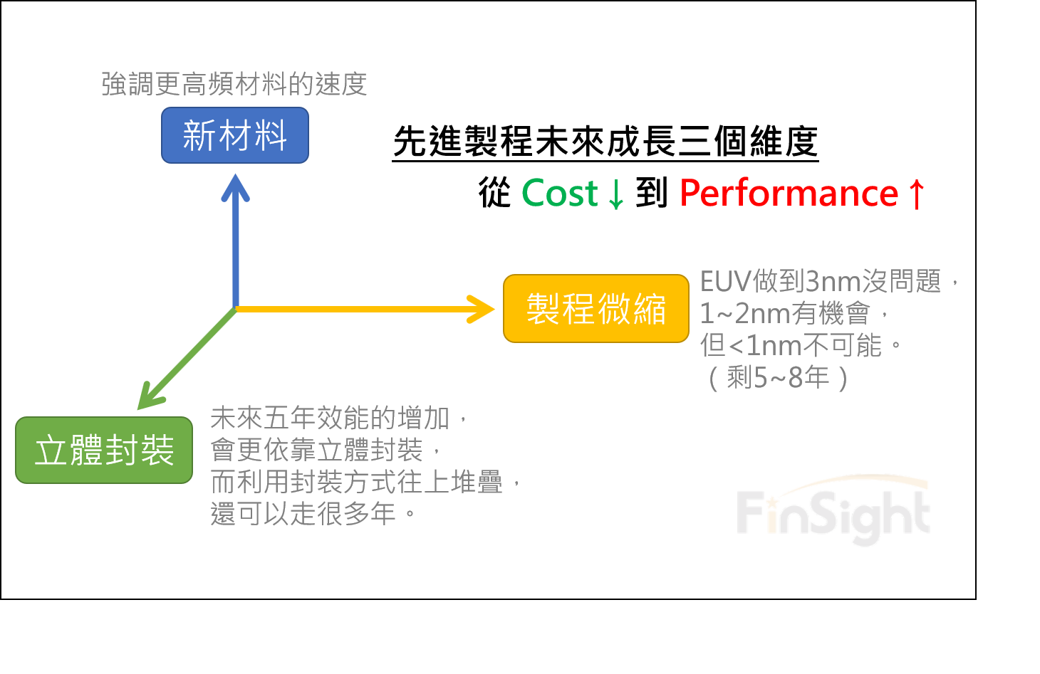
There are three main ways to raise chip performance: process scaling, 3D packaging, and new materials.
Heterogeneous 3D packaging takes chips of different types and integrates them with system level 3D packaging technology. It raises performance and cuts power, and it demands serious integration capability from the manufacturer.
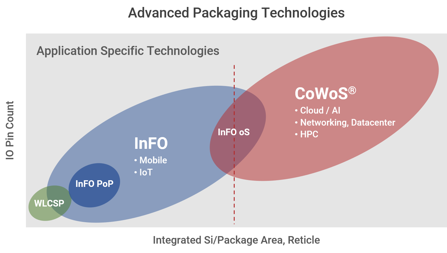
Split advanced packaging by application and you get two main buckets.
- Consumer products: TSMC's InFO packaging went into the A10 chip in the iPhone 7 starting in 2017, and it was the reason TSMC beat Samsung and took the order on a sole source basis.
- High performance computing products: AMD, NVIDIA and Xilinx use TSMC's CoWoS packaging in their data center products, and the cloud and AI trend has created a lot of demand for it.
Consumer products want compute performance too, but they also have to be thin, light, small and reasonably priced. So the main use today is Apple's own processor, and penetration elsewhere is still low.
Other packaging houses are pushing hard into high density fan-out as well. ASE and Powertech, Taiwan's packaging and test houses, along with Samsung, are building wafer level and panel level fan-out lines. Competition there is getting tougher.
High performance computing chips are the opposite. They are judged on performance and power rather than size, and they mostly sit in data centers. With the chase for advanced process nodes, chip sizes getting larger, and the CoWoS silicon interposer being extremely hard to build, packaging houses face a very large barrier to entry. This is where TSMC is strong.
Weighing the market and the competition, we prefer advanced packaging tied to high performance computing chips.
3DFabric: the advanced packaging platform TSMC launched at its technology forum
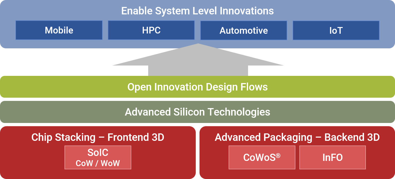
At the August 2020 technology forum, TSMC introduced 3DFabric, an advanced packaging platform that pulls together its 3DIC technologies including SoIC, InFO and CoWoS. Stacking dies and pulling memory into the package is aimed squarely at AI workloads.
We think 3DFabric creates a large lead for TSMC, for two reasons.
- Front-end plus back-end packaging changes the rules of chip design. As advanced process nodes get more expensive, 3D stacked packaging has to be considered in the chip design from the development stage. Whether the customer uses a chiplet design, meaning one large design split into several small dies, or front-end 3D, it forces TSMC and the customer to design the chip together, which is a stickier relationship than a foundry usually gets. That is what vertical integration from design through packaging actually buys.
- A customizable open platform helps customers adopt the new technology. With this many value-added technologies in hand, TSMC needs a dedicated platform to help customers see what designs the new technology fits. An open platform makes it far easier to get the technology into real products.
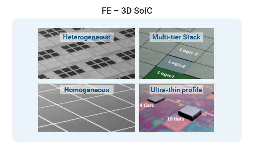
Inside 3DFabric, TSMC splits packaging into a front-end stage and a back-end stage.
- Front-end 3D: SoIC integrates homogeneous or heterogeneous chiplets on the wafer into something that looks like a single system on chip (SoC), with a smaller area and a thinner profile. From the outside the new chip looks like an ordinary SoC, but the heterogeneous integration the customer needs is embedded in it. Front-end packaging has to be baked in from the first architecture review. Because it is fundamentally the act of building an SoC, only a wafer fab can do it, and it cannot stand alone: it has to be paired with back-end packaging and test.
- Back-end 3D: an SoIC die that has come out of front-end packaging still has to be paired with the existing 3D packaging technologies, such as TSMC's CoWoS and InFO. Back-end packaging is also the area other packaging and test houses are pushing into, so it is not necessarily a fab-only business.
Figure 4 makes the point: a chip built with SoIC takes the place of what used to be the SoC, rather than replacing one of the other packaging steps. That is exactly why the discussion with the chip design house has to start at the design stage, during development.
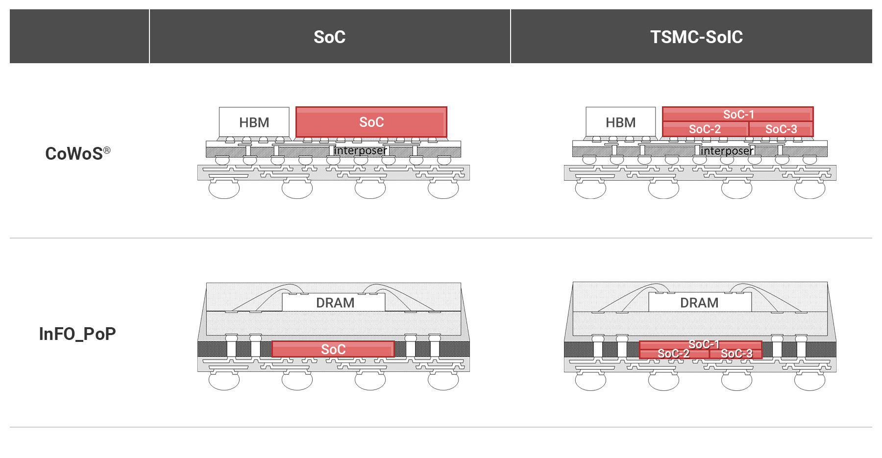
Once SoIC can be commercialized and used in end devices, Mark Liu's point will look right: semiconductor technology from here has to be described in terms other than the nanometer node. His other line: anyone counting the march from 7nm to 5nm to 1nm is watching the wrong number.
There is no SoIC product on the market yet. If one arrives, TSMC's lead takes a large step up.
So the question we should care about is which applications will need a product like this.
Bottom line: advanced packaging is where semiconductor technology moves next
With advanced packaging becoming the key to optimizing the product, TSMC ends up as the integrator in the vertical supply chain. It has to run everything from front-end design to back-end packaging and hand the customer one integrated service.
TSMC has also been expanding packaging capacity aggressively. We expect the advanced packaging capacity coming on over the next two years, paired with 7nm, 5nm, 3nm and the nodes after them, to build a firmer technology moat.
The next post, After Moore's Law, TSMC's 3D Packaging Builds an Absolute Lead, Part 2: Who Pays the Bill, turns to customer demand for advanced packaging and our overall investment view on TSMC.